Cleanroom Facility Basel
Welcome to the D-BSSE Cleanroom Facility. With state-of-the-art tools and comprehensive processing knowledge, we offer the scientists means to fabricate complex microsystems, microelectromechanical systems (MEMS), and microfluidic systems.
Our mission:
- Provision of tools and processes to fabricate complex micro- and nanostructures
- Support of users with project-specific consulting and process development
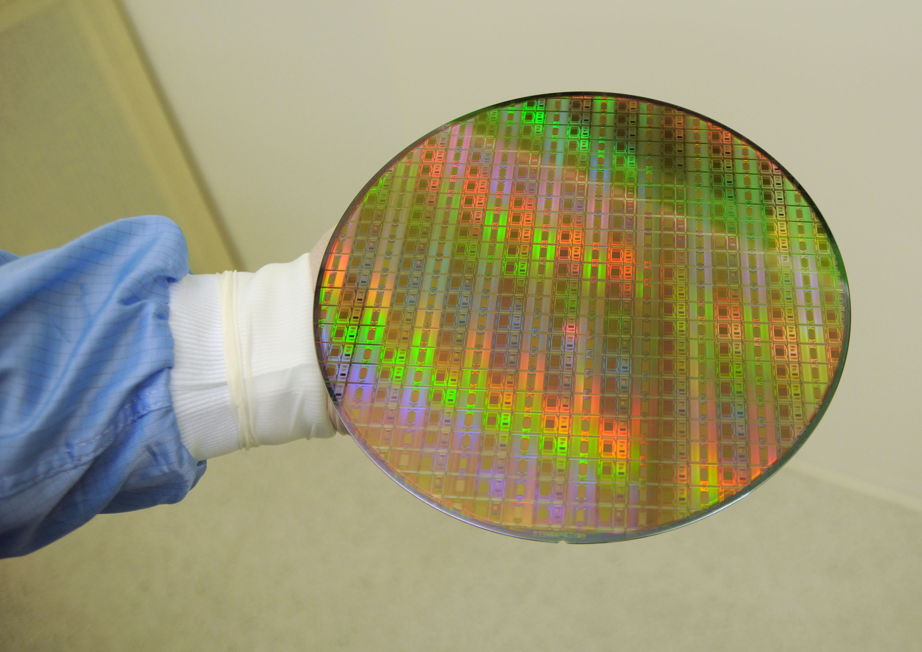
As one of the first research cleanroom facilities in Switzerland, we have the capabilities to process substrate sizes up to 8 inches (200 mm) diameter.
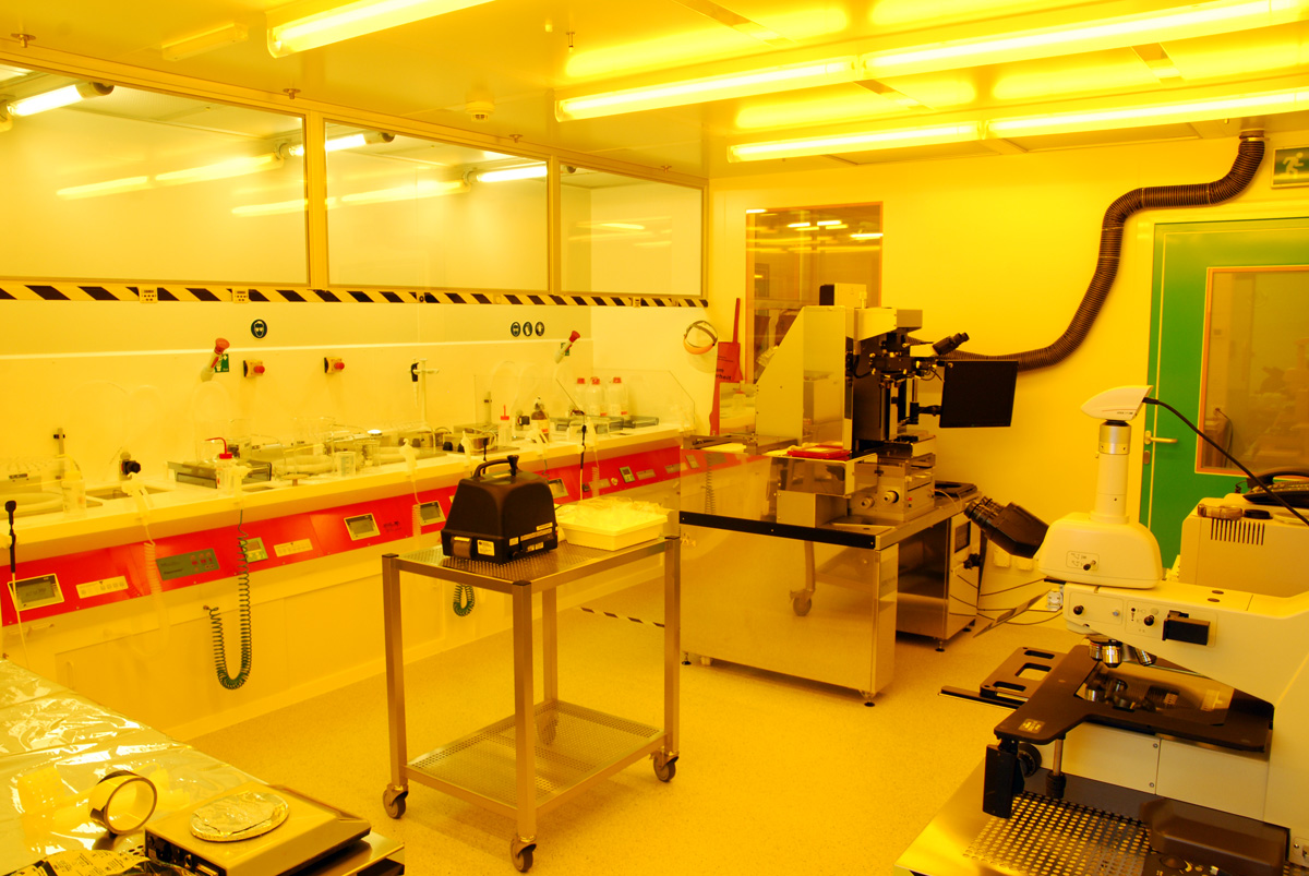
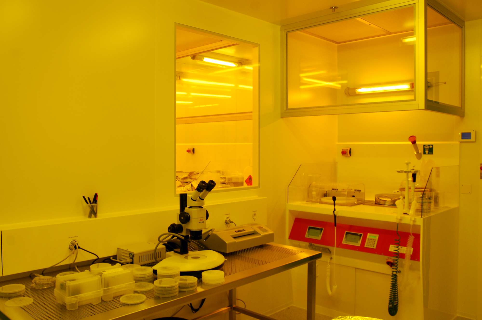
Equipment
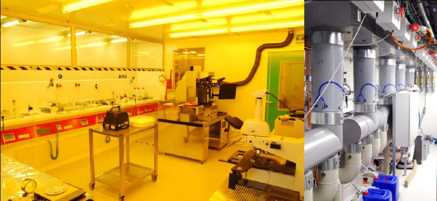
The cleanroom facility is equipped with state-of-the-art tools to perform thin-film deposition, etching processes and lithography (proximity and contact printing) with good reproducibility to fabricate complex microsystems.
Dry processing
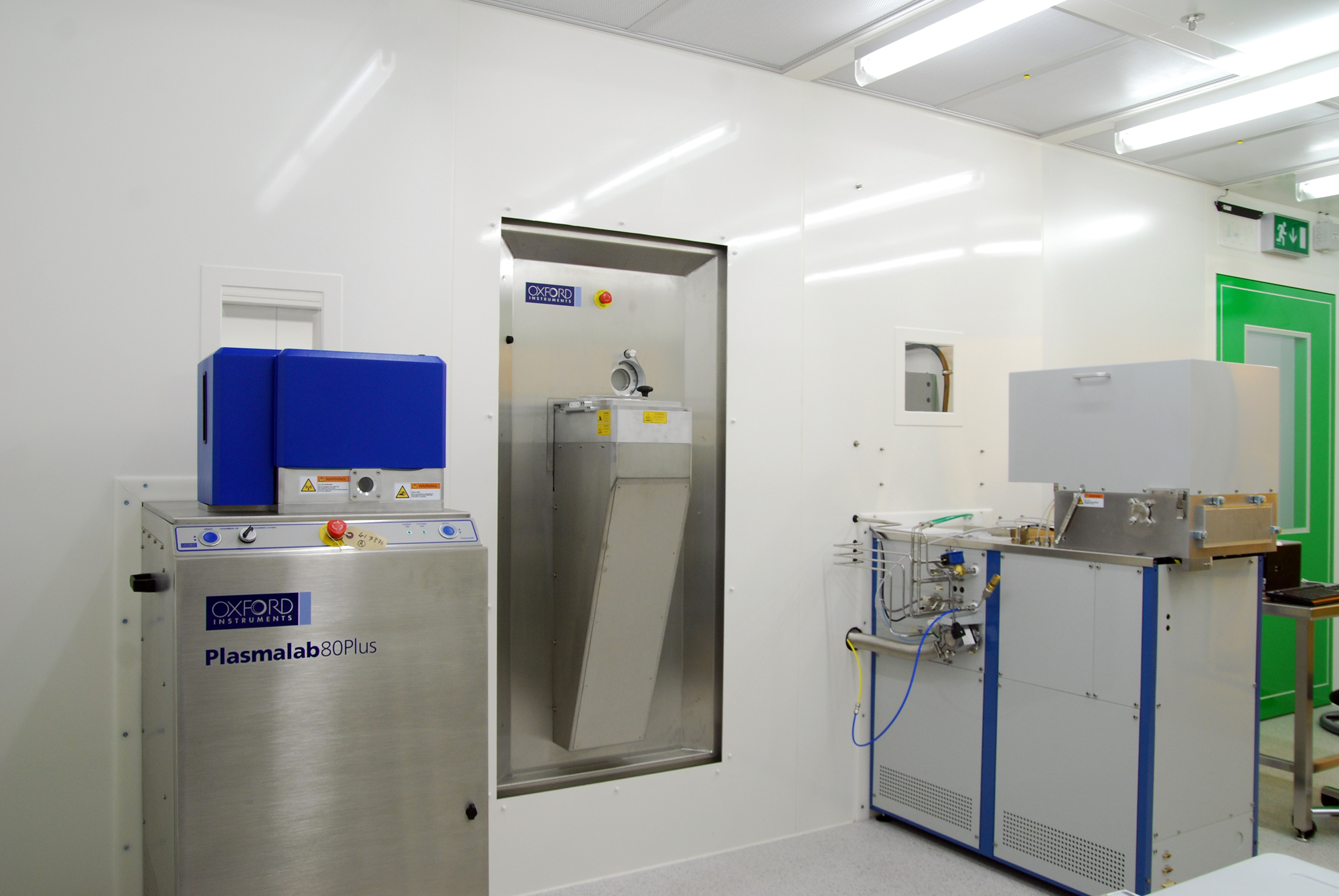
Oxford Instruments Plasmalab 80+:
- Plasma Enhanced Chemical Vapor Deposition (PECVD)
- Deposition of SiO2, Si3N4, SiOxNy films
Oxford Instruments Plasmalab 100:
- Reactive Ion Etching (RIE) and Deep Reactive Ion Etching (DRIE)
- Etching of Si, SiO2, Si3N4, SiOxNy and organic materials
- Fabrication of high-aspect-ratio structures in silicon.
- Inductively-Coupled Plasma (ICP) option for up to 4 inch wafers
Oxford Instruments Ionfab 300LC:
- Ion Beam Deposition (IBD) and Ion Beam Etching (IBE)
- Deposition of metallic and nonmetallic materials
- Etching of metallic and nonmetallic films and substrates.
- Very good uniformity (etching and deposition)
Microwave plasma asher:
- Removal of photoresist masks and surface activation
Wet processing
Goller Reinraumtechnik wet benches:
- KOH bath (temperature controlled) for anisotropic silicon etching
- BHF bath (room temperature) for SiO2 etching
- Quick-dump-rinse bath for de-ionized water rinsing
Lithography
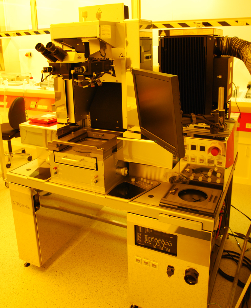
Karl Suss MABA8-Gen3 mask aligner:
- 1:1 pattern transfer from glass or foil masks (contact and proximity printing)
- Broadband illumination (350 – 450 nm wavelength)
- Alignment accuracy of 0.25 µm; optical resolution down to 0.5 µm
Goller Reinraumtechnik lithography wet benches:
- Substrate cleaning (Ultrasonic de-ionized water bath, Spin rinse dryer, QDR bath)
- Hotplates for dehydration, priming, soft and hard baking
- Spinner for developing and resist stripping
Polymer processing
- Separated area for polymer processing to avoid contamination of other processes.
- Spin coater, hotplates, degassing chamber: SU-8 and PDMS layer formation, casting and molding, packaging
Inspection and analysis
Optical microscopes:
- Nikon and Zeiss inspection microscopes
- Leica DM6000 chip scanning microscope
Surface and film analysis
- Veeco Dektak 150 stylus profilometer: film thickness and stress measurements
- KLA Tencor AlphaStep 200: film thickness measurements
- Four-point probe: resistivity measurement of metal films and semiconductors.
- Zeiss Axiotron: optical film thickness measurements
- Wafer prober: electrical tests on wafer level
Packaging
- ESEC 3088i Wire bonder: manual and automatic wire bonding
- Kulicke & Soffa 4526 manual wire bonder
- Flip-chip bonder
- Ultron Dicing-tape laminator
- Disco DAD3240 dicing saw
- Disco DCS1440 cleaning system
Meet the Team
Mattenstrasse 26 Mattenstrasse 26
4058 Basel 4058 Basel
Switzerland Switzerland
+41 61 387 34 17 +41 61 387 32 12
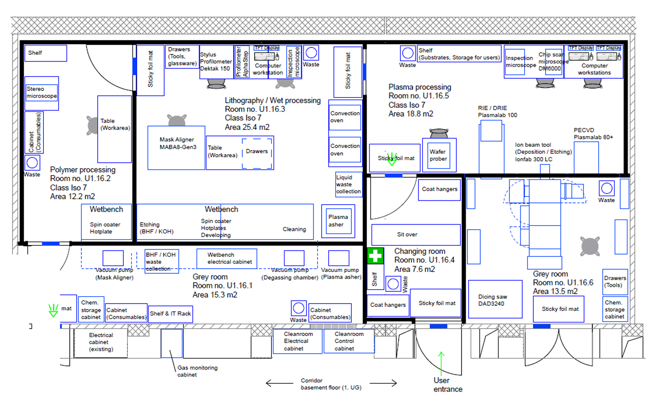
Floorplan of the Cleanroom Facility