Analytics
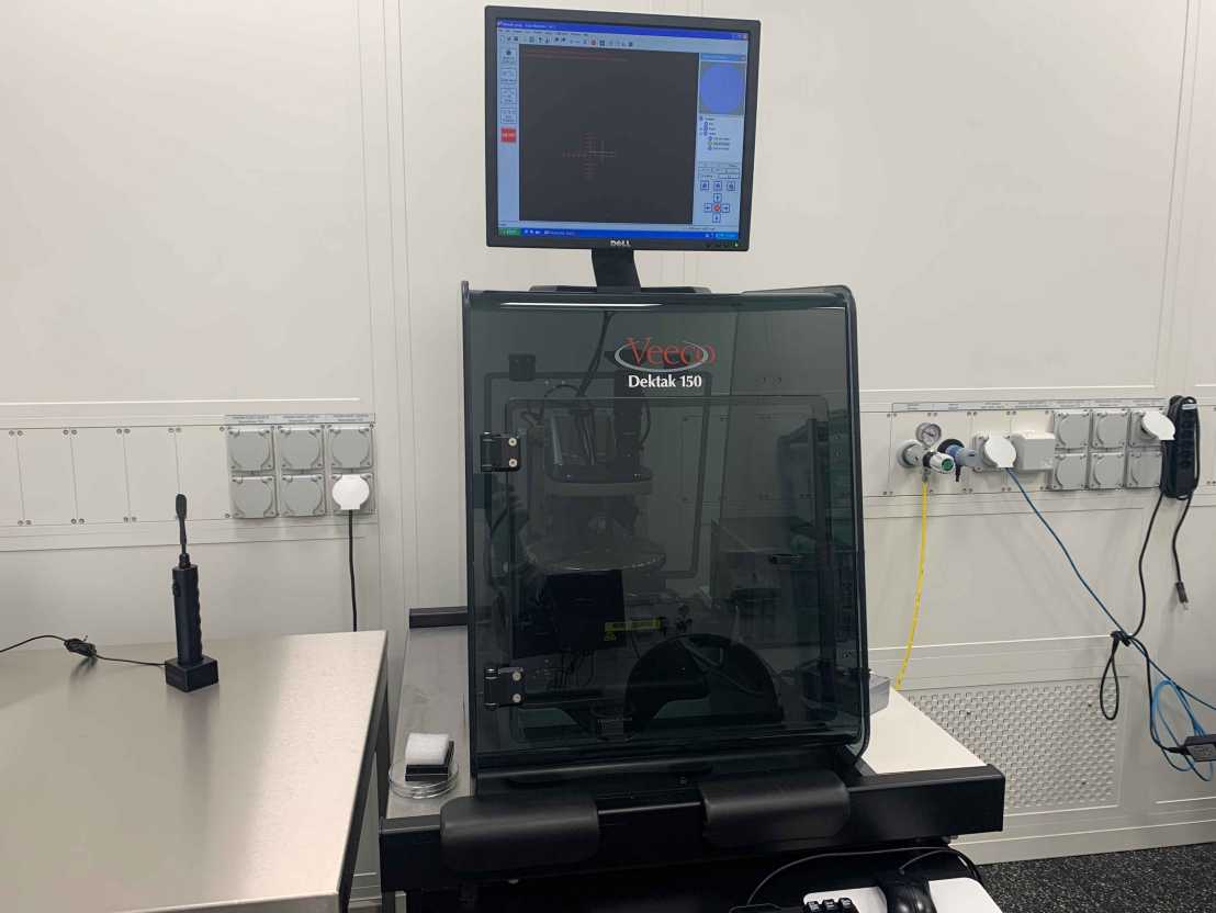
The Veeco Dektak 150 stylus profilometer is a fast tool for measuring surface profiles and step heights in the micro and nanometer range.
- Contact profilometer with nanometer accuracy
- Compatible with samples up to 200 mm (8 inch) diameter
- Maximum step height 1 mm

Filmetrics F20 Thin Film Spectrometer
Filmetrics F20 Thin Film Spectrometer, a spectroscopic film-thickness measurement system
- 15 nm - 70 µm thickness range
- Measurement of refractive index
- Large material library avaliable

Keyence VK-X 3000 confocal laser scanning microscope
Keyence VK-X 3000 Confocal Laser Scanning Microscope
- 3D profilometry via confocal laser scanning, focus variation and white-light interferometry
- Sub-nanometer z resolution
- Film-thickness measurement
- Automated measurements and stitching
- Powerful analysis software
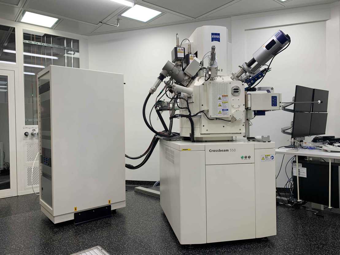
The ZEISS Crossbeam Large Chamber Scanning Electron Microscope (SEM) is a cutting-edge instrument designed for high-resolution imaging and detailed material analysis. Up to 8 inch wafers can be loaded.
The large chamber is equipped with:
- Load lock for fast loading of substrates up to 8 inch in diameter
- Focused Ion Beam (FIB)
- Gas Injection System (GIS)
- Energy Dispersive X-ray Spectroscopy (EDX)
- Scanning Transmission Electron Microscopy (STEM) sensor
- Detectors: SE2, BSD, ESB, InLens
- Plasma cleaner